domingo, 25 de julio de 2010

CERa/CERb Coeficientes de transferencia de masa y difusión

Se han diseñado dos aparatos de laboratorio independientes para permitir a los estudiantes medir difusividades moleculares y, al hacerlo, familiarizarse con las nociones básicas de la teoría de la transferencia de masa. El aparato de difusividad gaseosa (CERa) trata de la difusión con el flujo global, y el aparato de difusividad líquida (CERb), de un proceso de contradifusión equimolar.
CERa
Aparato montado en banco para la determinación de coeficientes de difusión de un vapor en aire, que utiliza el método de medir la velocidad de evaporación de un líquido a través de una capa estancada a un flujo de aire, y que consta de:

1) Un tubo capilar con diámetro interior preciso, que puede ser llenado con una jeringa, y en cuya parte superior se proporciona un medio para pasar un flujo de aire (o un gas inerte) para eliminar el vapor.
2) Una bomba de aire.
3) Un microscopio móvil con ajuste de enfoque de precisión y montado de tal forma que se desplaza verticalmente contra una escala con nonio con graduaciones de 1,0mm.
4) Un baño de agua con control termostático, en el cual se coloca el tubo capilar, capaz de mantener un control preciso sobre la temperatura, desde temperatura ambiente hasta 60 grados centígrados, con precisión de ±1 grado centígrado.


Posibilidades experimentales:
> Medición directa de velocidades de transferencia de masa en ausencia de efectos de convección.
> Uso de las leyes de los gases para calcular diferencias de concentración en términos de presiones parciales.
> Uso de la ley de Fick para medir coeficientes de difusión en presencia de un gas estacionario.
> Medición del efecto de la temperatura en los coeficientes de difusión.
> Familiarizarse con el uso de instrumentos de laboratorio para obtener mediciones precisas de datos requeridos para el diseño de procesos industriales.

CERb
Aparato montado en banco para la determinación de coeficientes de difusión de componentes en fase líquida. El método utiliza una célula de difusión de tubos capilares, construida de tal forma que permite una contradifusión equimolar entre líquidos de diferente concentración en cada lado de la célula sin que se produzcan efectos de convección.

Los cambios de concentración producidos con respecto al tiempo en un lado de la célula son medidos con el sensor de conductividad y el medidor suministrados, y un agitador magnético mantiene bien mezclada la solución.

La resolución del sensor de conductividad y el medidor es de 0,1 x 10⁻⁶ S para una solución salina de 1M con difusión a agua pura.

Es posible obtener valores de difusividad precisos y reproducibles en un periodo de 1,5 horas de prácticas en el laboratorio.

Posibilidades experimentales:
> Medición precisa de velocidades de transferencia de masa en ausencia de efectos de convección.
> Uso de las leyes de los gases para calcular diferencias de concentración en términos de presiones parciales.
> Uso de la ley de Fick para deducir coeficientes de difusión a partir de mediciones de la velocidad de transferencia de masa y la diferencia de concentración.
> Análisis sencillo de un proceso de estado inestable de primer orden.
> Efecto de la concentración en los coeficientes de difusión.
> Familiarizarse con el uso de instrumentos de laboratorio para obtener mediciones precisas de datos requeridos para el diseño de procesos industriales.

Accesorio de registro de datos (opcional). Permite que las señales del medidor de conductividad usado en la célula de difusión sean visualizadas, registradas y guardadas en una PC suministrada por el cliente, usando un interfaz USB.

Asignatura: EES
Fuente:http://www.discoverarmfield.co.uk/data/esp/cer/?js=enabled
Ver: http://diffusioninsolidsees.blogspot.com/

Applied technology

Nanotecture’s combined expertise in electrochemistry and nanotechnology has given rise to a range of unique nanoporous materials with special electro-chemical properties. These have been successfully applied to the development of high-performance electrodes and supercapacitors.Of particular relevance to electrical energy storage is Nanotecture’s nanoporous nickel (II) hydroxide [Ni(OH)2] material. This is produced in a modified version of Nanotecture’s liquid crystal templating process, with the facility to modify and enhance the electrochemical behaviour of the underlying material to suit particular applications. Capable of discharging up to 50% of its charge in under 0.5 seconds compared with over 15 seconds for a non-porous equivalent, this nanoporous nickel (II) hydroxide lies at the heart of Nanotecture’s high-performance electrodes and supercapacitors.

High performance supercapacitorsNanotecture’s high-performance supercapacitor design marries the power and cycle-life benefits of a carbon-carbon supercapacitor (also known as an ultracapacitor) with the energy storage characteristics of a battery. The resulting device, known as an asymmetric hybrid supercapacitor, is capable of significantly outperforming standard supercapacitors in terms of both specific energy and specific power. This unique device - which owes its name to the asymmetric capacities of the two electrodes and the presence of two different charge-storage chemistries in the same design - combines Nanotecture’s high-performance nanoporous nickel (II) hydroxide electrode with a carbon counter-electrode. The former stores charge like a battery whilst the latter stores charge like an electrochemical capacitor.


The benefits of the nanoporous nickel (II) hydroxide electrode are twofold. The significantly greater surface area of the nanoporous material provides high energy storage capability whilst the very much shorter solid state diffusion paths greatly speed up the charging/discharging process. The result is a device capable of delivering more energy at higher powers and at faster rates than a standard electrochemical supercapacitor. Unlike other battery technologies, Nanotecture’s technology uses an electrolyte that is water-based, non-toxic and non-flammable. In addition the materials are not nanosized particles but micron-sized particles with nano-pores, making them easier and safer to handle.

Asignatura: EES

Solid state fabrication of Metal Matrix Composites

Solid state fabrication of Metal Matrix Composites is the process, in which Metal Matrix Composites are formed as a result of bonding matrix metal and dispersed phase due to mutual diffusion occurring between them in solid states at elevated temperature and under pressure.

Low temperature of solid state fabrication process (as compared to Liquid state fabrication of Metal Matrix Composites) depresses undesirable reactions on the boundary between the matrix and dispersed (reinforcing) phases.

Metal Matrix Composites may be deformed also after sintering operation by rolling, Forging, pressing, Drawing or Extrusion. The deformation operation may be either cold (below the recrystallization temperature) or hot (above the recrystallyzation temperature).

Deformation of sintered composite materials with dispersed phase in form of short fibers results in a preferred orientation of the fibers and anisotropy of the material properties (enhanced strength along the fibers orientation).

There are two principal groups of solid state fabrication of Metal Matrix Composites:

Diffusion bonding
Sintering
Diffusion Bonding
Diffusion Bonding is a solid state fabrication method, in which a matrix in form of foils and a dispersed phase in form of long fibers are stacked in a particular order and then pressed at elevated temperature.

The finished laminate composite material has a multilayer structure.

Diffusion Bonding is used for fabrication of simple shape parts (plates, tubes).

Variants of diffusion bonding are roll bonding and wire/fiber winding:

Roll Bonding is a process of combined Rolling (hot or cold) strips of two different metals (e.g. steel and aluminum alloy) resulted in formation of a laminated composite material with a metallurgical bonding between the two layers.

Wire/fiber Winding is a process of combined winding continuous ceramic fibers and metallic wires followed by pressing at elevated temperature.

Asignatura: EES

Implantation damage and transient enhanced diffusion modeling

Implantation damage controls most of the dopant diffusion effects seen in modern silicon technologies. Despite more than 20 years of effort, understanding of defect-coupled dopant diffusion still falls short of what is practically required to support state-of-the-art silicon technology development. To obtain models that are as predictive and efficient as possible, we must combine the best of our physical understanding with measurements of dopant profiles for technology-relevant conditions. This paper presents experimental results that provide insight into damage generation and annealing processes and discusses practical modeling approaches to support technology development.

Gains in performance and circuit density from ever smaller transistors motivate the continuing development of silicon IC technology. As transistor channel lengths decrease, the vertical and lateral dopant distributions in the source/drain regions must also scale to maintain acceptable device behavior. The majority of diffusion seen in most current process technologies is transient enhanced diffusion (TED) caused by damage generated during ion implantation. Disruption of the crystal lattice by collisions with the implanted ions also reduces channeling, modifying the dopant distribution for subsequent implants. Understanding the interactions between implantation and diffusion is central to submicron transistor technology.

Figure 1 shows dopant distributions in the source/drain region of a MOS transistor. During the tip and source/drain implants, ion collisions knock silicon atoms from their lattice sites, leaving a vacant lattice site behind and sending a new energetic silicon atom into the surrounding lattice. Secondary recoils generated by this atom create a cascade of displaced atoms of decreasing energy. Eventually the recoil atoms do not have enough energy to cause further displacements and come to rest as silicon self-interstitials. Some of the vacancy and interstitial point defects created by this process may recombine locally, but others remain as defect clusters. These dissolve during high-temperature annealing, releasing mobile point defects that control the diffusion of the implanted

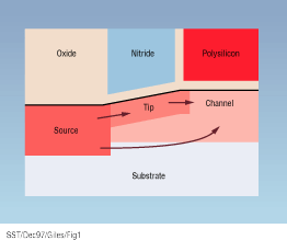
Figure 1. Implantation damage from the source and tip regions control transient enhanced diffusion throughout the structure.

ions as well as any other dopants that might be present. Since the point defect concentrations released are several orders of magnitude higher than the thermal equilibrium defect concentrations, dopant diffusivities also increase by several orders of magnitude. Eventually, recombination and trapping remove the point defects, and the dopant diffusivities return to normal. This phenomenon, TED, dominates dopant diffusion.

Since point defects diffuse rapidly, they can move from the implanted region into the channel, leading to additional diffusion there. Defect gradients can also drive channel dopant toward the surface, modifying the threshold voltage of the device [1]. The surface can act as a strong sink for dopant, modifying both the vertical and lateral diffusion. Amorphizing implants introduces further complications: solid phase epitaxial regrowth and the possible formation of a dislocation loop layer. The final doping profile results from the interactions among multiple dopant types and multiple implant damage generation and annealing cycles.

Implant damage creation
Implant damage creation is a complicated process involving the generation and recombination of recoil cascades and the formation of point and extended defects and dopant-defect clusters. Physically based modeling of this process is an active area of research, and is being addressed with a hierarchy of modeling approaches. Developing and validating these models is difficult; direct measurement of defect types and distributions is not possible in most cases. Significant progress has been made in recent years, using TEM to observe the time evolution of {311} and other extended defects [2], but these techniques provide information about the silicon after significant annealing, not after ion implantation alone, mixing implantation and diffusion effects.

Despite the complexity of the physical processes, the simplistic "+1" model [3] is surprisingly useful in providing initial conditions for point defect-based diffusion models. Figure 2 schematically shows recoil generation during ion implantation and recombination during the early stages of annealing. Although each implanted ion generates many interstitial-vacancy (Frenkel) pairs, bulk recombination removes the majority of them. Annealing also moves the implanted dopant atoms onto silicon lattice sites, displacing a single interstitial for each implanted ion. These "+1" interstitials have no corresponding vacancy with which to recombine, so they survive and influence dopant diffusion for much longer times.


Figure 2. Simplified model of damage generation and annealing resulting in the "+1" interstitial profile.

The model avoids detailed modeling of the implant damage process by making the starting interstitial profile the same as the implanted dopant profile. A scaling factor for the interstitial dose is often used as a fitting parameter, at least in part due to uncertainties in the other parameters of the diffusing system. Experimental measurements of interstitial dose trapped in {311} defects in the early stages of annealing support a scaling factor close to 1.0 [4]. The success of this approach implies that interstitial-vacancy recombination occurs rapidly, and the initial number of Frenkel pairs generated during implantation does not dominate TED.

Experimental validation of the "+1" model. The silicon surface is a very important recombination site during TED because it can act as an independent sink for both interstitials and vacancies. Distance from the surface determines how far defects must diffuse before being recombined [5] and strongly affects the annealing rate for damage. According to the "+1" model, the effective initial interstitial distribution (and so, TED) for two implanted profiles with the same implanted dopant distribution but different total damage should be the same. This claim can be tested experimentally by comparing samples implanted at different energies and tilt angles such that the as-implanted vertical doping profile is the same but the total damage created by the implant is different. Tilted implants allow investigation of different energies without varying the distance of the dopant from the surface.

Our experiments used phosphorus implants into [100] silicon through a 100-? screen oxide at doses equivalent to 5 ? 1013 cm-2 normal to the surface. We chose energy-tilt combinations of 100 keV at 7?, 148 keV at 50?, and 181 keV at 60? to produce as-implanted profiles that were as similar as possible. Monte Carlo ion implantation calculations of Frenkel pair generation for these conditions predicted increased interstitials and vacancies with increasing implant energy (Fig. 3). The annealing conditions, 800?C for one hour in an inert ambient, were chosen to be sufficient to anneal out the implant damage completely.

Figure 4a shows SIMS profiles before and after annealing. The as-implanted profiles are indeed similar, with the higher-energy implants slightly deeper and broader than the 100 keV implant. Although normal phosphorus diffusion is negligible under these annealing conditions, TED causes significant diffusion. To first order, the implants experience the same amount of TED and produce the same final phosphorus profile, validating the "+1" model assumption. On closer examination, the profile motion decreases slightly with increasing implant energy. Assuming a constant effective diffusivity, the diffusion lengths are 69, 65, and 60 nm for the 100, 148, and 181 keV cases, respectively. This difference may be due to a sputtering-induced increase in the net loss of interstitials for the higher implant tilt angles. Lower implantation energies of 30 keV (7?) and 62 keV (60?) produce the same behavior, coupled with a strong segregation of phosphorus to the silicon/oxide interface (Fig. 4b).

Implantation channeling profile measurements. When ions are implanted into a crystalline lattice in channeling directions, a certain fraction will travel large distances into the lattice with few nuclear collisions. These channeling ions produce a characteristic tail in the dopant profile. If the lattice is damaged, the probability of traveling large distances without nuclear interactions is strongly reduced. Therefore channeling can serve as a sensitive measure of the amount of damage present in the substrate [6]. Figure 5 shows how the channeling profile measurement (CPM) technique is applied. A 200 keV silicon implant with a dose of 1014 cm-2 and a beam current of 1 mA creates a damage profile. An annealing cycle at a particular time and temperature removes some of the damage from the wafer. Then, a boron channeling profile implant is made at 140 keV, 0? tilt, with a dose of 1013 cm-2. This implant creates a deep channeling tail for an undamaged wafer. Boron profiles for different damage annealing conditions illustrate the remaining damage. The technique is sensitive to silicon damage doses as low as 1013 cm-2, so small differences in remaining damage from higher dose implants can be detected.
The "+1" model requires that most of the Frenkel pairs generated in the collision cascades rapidly recombine during the earliest stages of the anneal, while the wafer temperature is ramping up to the target anneal conditions. Figure 6 shows the effect of annealing the silicon damage for 5 sec and 20 sec at 600?C. Even at this low temperature, a large recovery of the implant damage occurs within 5 sec, leaving some residual damage that appears to be stable at 600?C. The very rapid recombination of the initial damage cascade implies an extremely small energy barrier to interstitial-vacancy recombination.

CPM can also measure the stability of the residual damage at higher annealing temperatures. Figure 7 compares anneals for 10 sec at 600 and 900?C, showing a second stage of damage recovery. The 900?C boron profile is very close to the undamaged case. However, the observation of TED over a few minutes at these temperatures means that excess interstitials must still be present in some form. The staged nature of damage recovery can lead to multiple bursts of TED at different anneal temperatures, as discussed below.
Transient enhanced diffusion
Understanding of the physical mechanisms controlling TED has made great progress in the past few years by building on a basic understanding of defect behavior and dopant-defect interactions [7, 8]. Experimental evidence has verified the strong correlation among {311} defects, dopant-interstitial clusters, and TED. Physical models with different levels of complexity have been shown to give good agreement with experiment, but comparisons are usually limited to a small number of implant/anneal combinations. While this approach is entirely appropriate for the development of physical understanding, modeling for technology development must account for all the implantation and annealing steps in a technology flow. This section examines some of the challenges of modeling for technology development, focusing on conditions typical of the tip region doping in a MOS device.

TED across multiple anneals. Annealing steps include both the deliberate high temperature anneals designed to drive in and activate dopant, and the incidental, lower-temperature anneals associated with the deposition of some material layers. At lower temperatures, repairing implantation damage takes longer, so TED extends for a longer time. This effect can increase total dopant diffusion as annealing temperatures are reduced: the lower-temperature steps dominate the final dopant profile. The low energies and high doses used in modern technologies have more complex interactions than this simple view would suggest, making it harder to predict the outcome of a multitemperature anneal sequence.

The implant was made at 5 keV and 0? tilt into bare silicon at a dose of 1015 cm-2. The profiles display several interesting characteristics. First, the peak shows a displacement toward the surface and a decrease in dose during the first annealing step. This effect is discussed in the next section. Second, TED at 650 and 750?C appears to be complete after 90 min, but a subsequent RTA step causes a second burst of TED and additional profile motion. The second TED phase is complete in <10 href="javascript:OpenLargeWindow(265014,650,666,">
Relating these results with the CPM results described earlier, the implantation damage appears to form defects with several different annealing temperature thresholds. Annealing at an intermediate temperature produces a burst of TED as some categories of defects dissolve, but other defects may cause a further burst of diffusion when a higher-temperature anneal occurs. For high-concentration arsenic implants, arsenic-vacancy cluster formation may inject additional defects [9]. These clusters form during deactivation from the highly activated state left by epitaxial regrowth of the amorphized surface layer.

Dopant redistribution and solubility effects. The silicon/oxide interface is a strong sink for dopants as well as point defects. When trapped in the oxide, the dopant is electrically inactive [10] and is removed when the oxide is etched away. This behavior, observed for phosphorus, boron, and arsenic, can result in the loss of half or more of the implanted dopant. The effect is clearly visible in Fig. 4b, which shows SIMS profiles for annealed phosphorus before and after the surface oxide was removed using HF. The profile after etching contains only 50% of the original implanted dose. Surface loss can also significantly reduce lateral dopant motion near the surface at a mask edge, a critical region for technology applications.

The dose loss effect is linked to TED because the large transient diffusivity allows rapid transport of dopant to the interface. After amorphizing implants, solid phase epitaxial (SPE) regrowth may induce a partial sweeping out of dopant from the regrown layer. For example, in Fig. 8, the lowest-temperature anneal shifts the arsenic peak toward the surface and reduces the total arsenic dose. Since SPE occurs rapidly at temperatures above 500?C, we expect it to be completed during the temperature ramp-up period as wafers are pushed into the furnace.

For boron, an additional important effect is reduction in effective boron solubility during the transient [11], due to the formation of boron-interstitial clusters [12]. Figure 9 shows experimental measurements for annealing of BF2 and B implants. The BF2 example was implanted through a 130? oxide at 45 keV to a dose of 2.5 ? 1014 cm-2 and annealed at 900?C. The B example was implanted at 40 keV through the same oxide to a dose of 2 ? 1015 cm-2 and annealed at 800?C. For short anneal times, TED is in progress and the profiles show a characteristic kink near the intrinsic carrier concentration [13].

Modeling for technology development
Early dopant diffusion modeling in silicon was based on work [14] that interpreted the Fermi level dependence of diffusivity as a consequence of the equilibrium behavior of charged point defects. To extend this interpretation to the far-from-equilibrium conditions induced by ion implantation, a model must include the creation and evolution, in both time and space, of the relevant defect types and their interaction with free dopants and defects. The most straightforward approach, the so-called fully coupled approach, is to solve the continuity equations for the various defect types while also solving dopant diffusion. This approach is simple, direct, physical, and has the greatest possibility of being predictive across a wide range of process conditions. The three major drawbacks of the fully coupled approach are: lack of well-accepted physical mechanisms spanning the full range of conditions of technological interest for both implant damage creation and dopant-defect interaction; computational cost; and the difficulty of calibrating a complex and strongly coupled model system.

Given the limitations and costs of the fully coupled system and the need for calibrated models that keep pace with technology development, we have decided to use a hierarchical approach. Exploration of defect physics and evaluation of new defect models requires solutions of the coupled system. For day-to-day technology development, however, the best approach uses the one dopant diffusion equation system, obtaining an effective dopant diffusivity from a model for implant damage annealing in time and space. A semi-empirical implant species/energy/dose dependent damage creation/accumulation model provides the initial conditions.

Our effective diffusivity model represents implant damage by a dimensionless quantity representing an effective damage dose. Analytic distribution functions incorporate spatial effects, allowing, for example, dopant up-hill motion driven by the defect gradient near the surface. The effective damage dose decreases during annealing with limited amounts of the total damage available for repair at lower annealing temperatures. The dopant diffusivities are greatly enhanced while the damage clusters are dissolving and sharply drop back to the intrinsic values when the damage is annealed out (Fig. 10). While a clear physical picture is still needed to develop useful forms for the damage annealing models, the practical dependence of the simulation on details of the underlying physical mechanism is much reduced. When technology development demands capability in a brand-new application area or revolutionary progress has been made in physical understanding, the effective diffusivity model offers greater flexibility and extensibility, as well as a much shorter turn-around time for modification and calibration. Figures 11 and 12 show example effective diffusivity calculations based on experimental results presented earlier. We include dose trapping and re-emission from the silicon/oxide interface [15], and the effect of dopant redistribution during SPE. Good agreement can be found for simulations of complex implant/anneal sequences of technological interest.

Asignatura: EES

Silicon rectifiers and Silicon power transistors

In 1957 the production quantity of US transistor has reached 30 millions, compared to 0.6 million at 1952, similar to tube production quantity at 1952. Actually the semiconductor progress of first 10 years is more than the tube progress of first 25 years, said by Kelly of Bell Lab. Transistor has been used everywhere, and the growth of complex electronics system, such as computer, telephone switching system and space/military applications pushing transistor to more integrating form---solid circuits(later name as integrated circuit) prototype in 1958 by Kilby of TI, but it is germanium. All the practical integrated circuits are manufactured by silicon planar technology, which is after Noyce of Fairchild in 1959. This story is just like true transistor(junction type) invented in 1949 not point-contact transistor invented on December 1947.


In 1958 Fairchild marketed their first silicon diffusion mesa transistors to RCA, and then planar transistor in 1959. In early 1960s the epitaxial growth technology is invented. The planar silicon dioxide passivated and epitaxial growth manufacturing processes are the same as silicon diffusion technology as the foundations of modern solid state device. The other important semiconductor manufacturing process---ion implantation(can give the most precise control of impurity profile) is practical in 1970s.


With excellent semiconductor manufacturing technology the old(1945) idea of FET successful fabricated in 1961 at Fairchild, and it is MOSFET used in any large scale IC. But MOS IC was not really took off until late 1960s, all 1960s are still bipolar IC territory. The DIP apckage is introduced by Fairchild in 1965, soon adopted by other semicondcutor companies, the plastic package for all other semiconductors also.

In 1967 Sporck, general manager of Fairchild resigned and take four key man to reorganize National Semicondcutor(founded at Connecticut in 1959 and moved to silicon valley in 1968)---famous for complete pheripheral IC line. In 1968 Noyce, R&D manager of Fairchild, Moore and Grove founded Intel---now it is the world's largest chip manufacturer, famous for complete processor lines(actually also famous for memory in the 1970s, but can not compete with asian semiconductor companies after 1980s, and also famous for network chipset.). In 1969 Sanders, market director of Fairchild and transferred from Motorola one year ago, took seven colleagues to form AMD, also famous for processor, memory and network chipset---strong competitor of Intel. In 1966 and 1967 there are three chip companies formed each, in 1968 there are 13 companies, in 1969 another 8 companies formed in Santa Clara Valley---that is the name of Silicon Valley come from.


In March 1961 Fairchild sold several kinds of IC to NASA. At the same time TI showed off midget computer made from 587 IC for computer of Air Force, which is only 1/150 volume and 1/50 weight of the same function transistor computer, which use 8,500 discrete solid state components. In this May President J. F. Kennedy announced that US will send a man to moon by the end of this decade, this aim has been fulfiled successfully but he can not see it by himself. This is only possible by IC which save a lot of space, weight and power. In 1962 the first communication satellite---Telstar, it's also impossible without IC, opening the satellite communication era. In 1964 Fairchild made the first linear IC---µA702, and then popular µA709 in 1965 and more popular µA741 in 1968, all are from Fairchild Semiconductor and all OP AMP IC---basic of all analog circuits.
Asignatura: EES

Parameters for hermetically sealed connectors

Sealing is a very complex science by itself as it involves many physical aspects, including mechanical design, materials science, surface science and fluid behaviour. Armin Reicharz reports.


For applications requiring hermetically sealed connectors - like vacuum processing equipment, pressure vessels or continually immersed devices - some parameters need to be carefully taken into account to achieve hermeticity.

Different levels of sealing exist. They should be adapted to the operating conditions, in which the equipment will be used. Installations having to withstand dust or water ingresses usually need to be environmentally sealed. Applications requiring gas tightness need a higher degree of protection; they are generally hermetically sealed.


To be referred to as hermetic, a system has to be designed to avoid its content leaking out or gas leaking in over an extended period of time. The effectiveness of a hermetic barrier is calculated in leakage rate values. Leak rates quantify the amount of gas flowing through the barrier every second and are expressed in mbar.l/s or atm.cm3/s. Hermeticity typically concerns leakage rates below 10-6mbar.l/s.


A typical hermetic connector requires several sealing barriers. Some advanced sealing techniques, like the ones developed by Fischer Connectors and described below, enable to exactly adapt the sealing performance of a connector to the level of protection it needs. To achieve such flexibility, each critical area of a connection - the panel interface, the contact block and the connectors interface - is protected by its own independent seal.

The panel seal (A ) is placed at the interface between the receptacle housing and the panel or equipment housing. It plays an important role for hermeticity because it covers a large cross section.
The protection of the contact block is ensured by a combination of two seals (B and C), a gasket sealing the junction between the contact block and the receptacle housing, and an advanced polymer compound covering the rear of the block and sealing the contacts.

Finally, the connectors interface is also protected by a seal (D). Not participating in making the system hermetic, it is dedicated to prevent ingress of water or harmful particles in the connecting area where male and female contacts mate.

Testing enables to guarantee that a connector is hermetic. For instance, all Fischer hermetic connectors are submitted to a 100 per cent quality screening test, using helium as tracer gas.

What are leakage and diffusion?
There are two majors mechanisms by which gas can get through a hermetic barrier: leakage and diffusion. Gas leakages are caused by material defectiveness, such as cracks and defects in the barrier. Even tiny, those imperfections ultimately result into the failure of the device. On the other hand, diffusion also called permeation is a natural process; induced by pressure difference, gas can migrate through solids, even without any defects in the barrier. Diffusion is generally known to occur in most plastics and rubber materials. Being a natural phenomenon, it can be limited but not fully eliminated.

The extent of both leak and diffusion mechanisms depends on the size and mobility of the gas molecules. For example helium molecules are very small and can easily penetrate even the tiniest cracks, while as a rule of thumb the penetration of Nitrogen (or air) is about one third of the helium value.

Material selection is very important in the design of hermetic applications. As explained above, the diffusion effect is correlated to the material used. Additionally, there is also another phenomenon linked to the nature of material: outgassing, also called desorption. Connectors are designed with many materials - such as insulating plastics, sealing resins or elastomeric seals - which naturally absorb a small quantity of water. Over time, or when environmental conditions change, the water molecules and other solution gases contained in the material itself are released. This is called outgassing and, while an environment is transformed in vacuum for example, it increases the gas load during the initial pumping phase. Heating the material can accelerate the outgassing effect.

To minimise both diffusion and outgassing effects, materials used in connector design have to be of high performance. Many materials were tested by Fischer Connectors Engineering team, and some - showing low permeation, outstanding chemical and high temperature resistances as well as low outgassing - proved extremely reliable. To achieve a leakage rate below 10-8mbar.l/s, Fischer hermetically sealed connectors are carefully engineered with state-of-the-art materials. For most receptacle seals, Viton - a fluoropolymer or FPM - is used as standard. The polymer compound used for the contact block sealing is epoxy resin.

Additionally, customised material solutions can also be developed for systems operating in very specific conditions.

The design and installation of the connectors play an important role in hermetic sealing. Indeed, gas can get trapped between assembled components. This gas, when getting released, causes what is called virtual leaks. Such virtual leaks typically result from air caught in bores, screws or between parts having large surfaces in contact.

Moreover, when installing a connector onto a hermetic system, it is important to check that no gas is trapped in the mounting area. Efficient panel sealing can only be achieved if the contact surface is correctly prepared. No excessive torque should be required to mount the connector, which generally implies the surface flatness to be <0.05mm.>
In conclusion, to ensure hermeticity and avoid leaking systems, the key parameters to consider are the exploitation of advanced connector sealing technologies, a careful selection of the materials used, optimised connectors designs and a precise installation. Manufacturers specialised in sealed connectors can contribute to the performance of hermetic equipments. Indeed, each project being different, a comprehensive analysis of the specifics of the application is highly recommended.


CVD Equipment Corporation "enabling tomorrow's technologies™"

Diffusion
P and N type dopant are typically diffused thermally into the substrate in a furnace at a high temperature and atmospheric pressure. The dopant source can be gases (PH3, B2H6), liquids (POCl3, BCl3), or solids (P2O5, B2O3 wafer pre-diffusion follow with a drive in step).
CVD Equipment provides single tube and multi-tube furnaces for batch wafer processes. The system can be configured for 4", 6" and 8" wafers with 10 and up to more than 100 wafers per load capacity to meet your research and production requirement.


Boat of wafers loading into Hot Wall Furnace Chamber

Oxidation

Silicon dioxide can be made by thermal oxidation of silicon wafers at a high temperature. The oxidation process can be produced by using 3 different methods depending on the film quality needed.


These methods are:


  • Dry oxidation using pure O2 gas at high temperature (around 1000 °C) produces high density and pinhole free oxide layer. Nitrous oxide can be used to produce oxynitride film.
  • Wet oxidation using O2 through a water bubbler occurs at 800 °C to 1100 °C. It produces lesser quality oxide but the oxidation rate is much faster.
  • Pyrogenic oxidation uses a separate heater to generate hot water vapor stream from the reaction of H2 and O2. It minimizes the temperature disturbance caused by the cool water vapor used in regular wet oxidation.

Here at CVD Equipment, we offer offer single tube and multi-tube thermal CVD for batch wafer oxidation processes.


12" raw wafers in boats before going into a CVD, LPCVD and many other process tools manufactured by CVD Equipment Corporation

Asignatura: EES

Fuente: http://www.products.cvdequipment.com/applications/diffusion/

Ver: http://diffusioninsolidsees.blogspot.com/

Unique Tystar Furnace Applications

Diffusion of Solid Source Dopants

Solid source dopant materials(Sb2O3, Zn3P2, and others) are sometimes required for many semiconductor process applications. For example, antimony diffusion into silicon is a desirable process for introducing slow diffusing n-type impurities into silicon. This process can be used for the formation of buried n+-layers for bipolar transistors or any other device structure, requiring a slow-diffusing n+-layer to minimize out-diffusion in subsequent heat treatment of the silicon wafer.

The most widely used antimony source material for Sb diffusions is antimony trioxide (Sb2O3). The Sb2O3 source material is placed into a separate source furnace with operating temperatures from 620 - 660ºC. At those temperatures the vapor pressure of Sb2O3 is sufficient for transfer of Sb2O3 vapor with a suitable carrier gas into the actual diffusion zone where the silicon wafers are located. The Sb concentration in silicon, or the sheet resistivity of the diffused Sb layer, which can be attained depends on:
  • Sb2O3 vapor pressure, or Sb2O3 source temperature
  • Silicon wafer or diffusion temperature
  • Diffusion time

Tystar Thermal CVD System


Antimony diffused layers with sheet resistivities of 10 to 60 Ohms/square or surface concentrations from 5 x 10¹⁸ to 5 x 10¹⁹/cm3 are typically attained.

Sb2O3 diffusions can be readily performed in the Tystar TYTAN diffusion furnace.
The diffusion temperatures are typically from 1230ºC to 1280ºC and require quartzware for high temperature operation. A thick-wall quartz tube is recommended. SiC wafer carriers and SiC cantilever rods are recommended to minimize quartz deformation at the higher temperatures. The gas inlet part of the process tube is extended beyond the actual diffusion zone and extends through a source furnace, which is attached to the diffusion zone heater. The source furnace consists of a small 3-zone heater, which extends into the skirt of the diffusion tube. It is essential that there is a smooth temperature transition from the source furnace to the diffusion zone. There can be no dip in the temperature or the Sb2O3 flux cannot be controlled. The temperature in the diffusion zone is controlled to < +/- 1ºC in the diffusion zone over a distance of 34”/860 mm, and in the source heater over a distance of 6”/150 mm.
The Sb2O3 material is introduced into the source furnace in a quartz boat, which is loaded from the gas inlet port of the extended diffusion tube. A tapered quartz flange or a ball joint is used to connect the gas inlet to the process tube. Process gases used for the Sb2O3 diffusion are either a combination of N2 with O2 or pure, dry argon. The Argon process minimizes the oxidation of Sb2O3 into Sb2O4, which has a much lower vapor pressure than Sb2O3 and results in a reduced consumption of Sb2O3. Several wafer loads can be processed with one charge of Sb2O3 in the source furnace. At the exhaust end of the process tube the Sb2O3 and Sb2O4 condenses and can present a particulate problem when the wafers are loaded and unloaded. A condensing cup is normally attached to the source end to capture the condensed Sb2O3 and Sb2O4. The Tystar TYTAN furnace offers a significant advantage for this problem. The patented heat plug design permits process operation at much reduced gas flows without back streaming from the scavenger. With proper provisions, minimal condensation is observed inside the tube resulting in much lower particulate generation.
  • Sheet Resistivity: +/- 5%
  • Oxide Thickness: +/- 3%
  • Junction Depth: +/- 5%

Asignatura: EES

Fuente: http://www.tystar.com/02_Furnace/diffusion.html

Ver: http://diffusioninsolidsees.blogspot.com/

Solid-State DNP-NMR Spectrometer 263 GHz AVANCE™ III

The world’s first commercially available solid-state DNP-NMR spectrometer.

1) DNP-Enhanced Experiments on Large Biological Systems
Dynamic Nuclear Polarization (DNP) experiments at 263 GHz/ 400 MHz provide a large gain in sensitivity and dramatic reduction in signal averaging time. This enhanced sensitivity enables researchers to study samples that otherwise would have been inaccessible to NMR such as certain membrane proteins or samples which are available only in very limited amounts or dilute concentration. A range of samples have been successfully enhanced on the new 263 GHz Bruker DNP spectrometer including small peptides, soluble proteins, membrane proteins, and large biological complexes. The DNP samples are prepared by adding a polarizing agent (such as e.g. TOTAPOL biradical to a shared solvent or alternatively by utilizing a native radical on the sample of interest. The samples are measured under MAS while at low temperatures, typically 100–120 K. Unmodified NMR experiments are performed while benefitting from continuously DNP-enhanced signal intensity through CW microwave irradiation.

2) DNP-Enhanced CPMAS of 13C-Proline
DNP-Enhanced CPMAS of 13C-Proline in Glycerol/Water with 20 mM TOTAPOL:25 μl sample, 1.5 mg U-13C-15N Proline, 8 kHz MAS, CPMAS with Spinal 64 decoupling, 110 k sample temperature, 8 seconds acquisition time for both microwaves on and off spectra


3) DNP-enhanced proton driven spin diffusion 13C-13C correlation experiment
DNP-enhanced proton driven spin diffusion 13C-13C correlation experiment on Barnase ribosome nascent chain complex with 10 mM TOTAPOL (nascent chain 13C labelled). 13 kHz MAS at 110 K. Experiment time: 17 hours. Sample courtesy of Hartmut Oschkinat, Leibnizinstitut fuer Molekulare Pharmakologie.


Asignatura: EES
Fuente: http://www.bruker-biospin.com/dnp-apps.html
Ver: http://diffusioninsolidsees.blogspot.com/

Development of models for the quantum-chemical treatment of crystalline solids and surfaces

Cyclic Cluster Model (CCM): In the CCM periodic boundary conditons are applied to large molecular clusters. In this way translationally equivalent atoms are guaranteed to have the same environment and becom indistinguishable. Boundary effects from atoms at the cluster borders are removed in the CCM.


The CCM can treat polymers, surfaces and solids. It has been shown that calculated properties converge rapidly with increasing cluster size, so that already medium-sized models describe bulk properties reasonably well. For ionic systems long-range Coulomb interactions are taken into account via the Ewald summation technique.

The CCM is related to the more commonly used supercell model (SCM) with restriction to k=0 except that the interaction are around each atom is not determined by an arbitrary cutoff threshold, but is defined by the Wigner-Seitz cell constructed by the translation vectors of the cyclic cluster. The CCM can be easily implemented in molecular codes at semiemipirical level, but it is also possible to modify an existing molecular density- functional formalism.


a) Application to problems in solid-state chemistry, surface chemistry, and heterogeneous catalysis. These studies are performed with semiempirical, density-functional and Hartree-Fock methods with the program packages CRYSTAL03, VASP, and MSINDO using the CCM and SCM. Recent activities of the group comprise


  • Effect of anion substitution on electronic properties, e.g. changes of optical transitions in the system ZnS/ZnSe
  • Point defect formation in solids, e.g. oxygen defects in Li2O, Li2B4O7
  • Effect of anion distribution in ternary systems, e.g. TaON and Zr2ON2


  • Surface structure of thin films, e.g. rutile on tungsten
  • Oxygen defect diffusion on surfaces, e.g. in the catalytically active TiO2 rutile(110) surface
  • Adsorption of small molecules and metal clusters on perfect and defective surfaces, e.g. NO/NiO, Pd2/TiO2, CO/SnO2
  • Molecular-Dynamics simulation of spectroscopic features of adsorbed molecules, e.g. H2O/rutile and oxalic acid/anatase.
  • Surface reactions of adsorbed molecules on surfaces, e.g. the DeNOx process on mixed V2O5/TiO2 catalysts o Electric field gradients for the identification of lattice sites, e.g. in LixTiS2.
  • Diffusion of small cations, e.g. Li at the interface region of nanocrystalline Li2O:B2O3 composites.
b ) Development of the semiempirical SCF-MO method MSINDO
  • Extension to elements of the fourth row transition elements Y to Cd.
  • Implementation of the CCM
  • Born-Oppenheimer molecular dynamics technique

  • Inclusion of higher multipole integrals
  • Parallelisation via SCALAPACK and BLACS

Asignatura: EES

Fuente: http://www.thch.uni-bonn.de/tc/index.php?section=forschung&subsection=bredow

Ver: http://diffusioninsolidsees.blogspot.com/